
The article offers a deeper understanding of the factors that impact on the silicon wafer flatness in the lapping process and also highlights the benefits of using a structured problem-solving methodology like Six Sigma.
Authors
Sanjeev P. Sahni, Principal Director, Jindal Institute of Behavioural Sciences (JIBS), O. P. Jindal Global University, Sonipat, Haryana, India.
Mithun Sharma, O.P. Jindal Global University, Sonipat, Haryana, India.
Shilpi Sharma, Assistant Professor, Jindal Global Law School, O.P. Jindal Global University, Sonipat, Haryana, India.
Summary
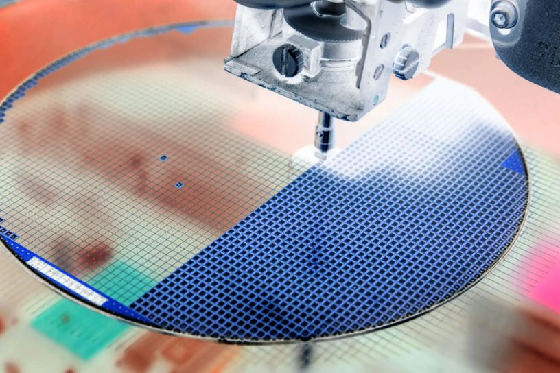
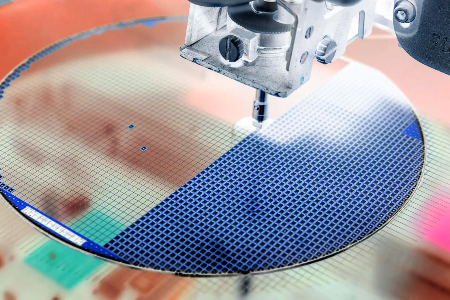
Aiming to reduce flatness (Total Thickness Variation, TTV) defects in the lapping process of the silicon wafer manufacturing, it is crucial to understand and eliminate the root cause(s). Financial losses resulting from TTV defects make the lapping process unsustainable. DMAIC (Define, Measure, Analyse, Improve and Control), which is a Six Sigma methodology, was implemented to improve the quality of the silicon wafer manufacturing process.
The study design and the choice of procedures were contingent on customer requirements and customised to ensure maximum satisfaction; which is the underlying principle of the rigorous, statistical technique of Six Sigma. Previously unknown causes of high TTV reject rates were identified, and a massive reduction in the TTV reject rate was achieved (from 4.43% to 0.02%). Also, the lapping process capability (Ppk) increased to 3.87 (beyond the required standard of 1.67), suggesting sustainable long-term stability.
Control procedures were also effectively implemented using the techniques of poka yoke and control charts. This paper explores the utility of Six Sigma, a quality management technique, to improve the quality of a process used in the semiconductor industry.
The application of the Six Sigma methodology in the current project provides an example of the root cause investigation methodology that can be adopted for similar processes or industries. Some of the statistical tools and techniques were used for the first time in this project, thereby providing new analysis and quality improvement platform for the future.
The article offers a deeper understanding of the factors that impact on the silicon wafer flatness in the lapping process. It also highlights the benefits of using a structured problem-solving methodology like Six Sigma.
Published in: Engineering Management in Production and Services
To read the full article, please click here.